|
|||||||||||||||||||||||||||||||||||||||||||||||||||||||||||||||||||||||
|
|
|
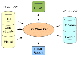
IO Checker verifies hundreds of pins in between FPGA and PCBWhen using large FPGAs on a PCB, making sure that the FPGA pins are connected to the right PCB signals is a cumbersome task. On the FPGA side, the pins are assigned to the HDL signals that form the toplevel of the logic implemented on the FPGA. On the PCB side, the pins have to be connected to the proper net that will connect it to other components on the PCB. Because implementation of FPGA and PCB is often done in parallel, the signal names used are not always identical. To make things even worse, it is often necessary to perform pin swaps to prevent PCB routing problems. These pin swaps have to be made both on the FPGA and the PCB. As this is almost always manual work, and current devices have over 1500 pins, a mistake is easily made.
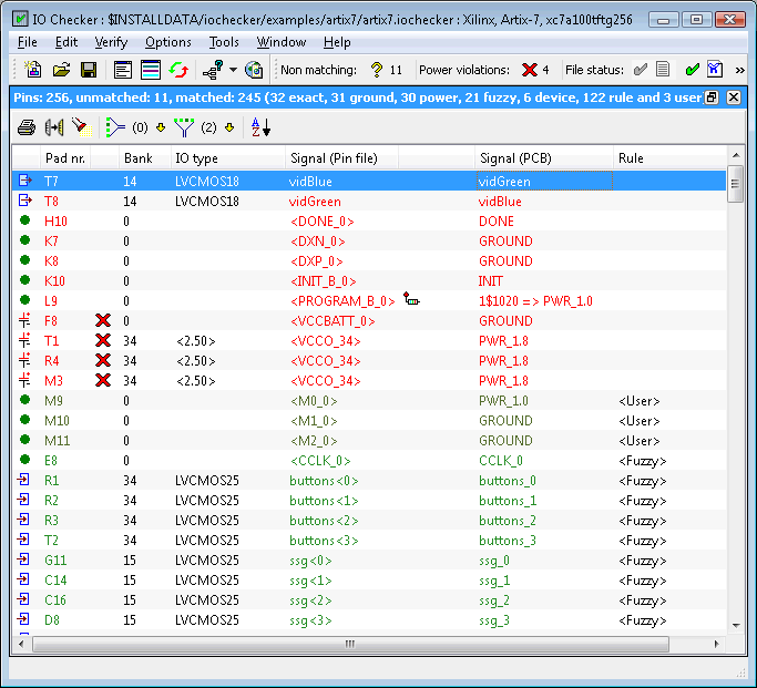
IO Checker offers an easy way to verify the PCB data with the FPGA data. Instead of comparing two lists with hundreds of pins manually, you can load the FPGA pin list file and the PCB netlist file in IO Checker. IO Checker will immediately recognize exact signal name matches and it will also use some fuzzy rules to handle common differences in FPGA and PCB signal names. In case different names were used on FPGA and PCB, IO Checker allows you to define regular expressions to match these names. Using regular expressions allows you to match groups of signals instead of having to check each signal separately. Once you have defined your rules and changes have been made on either the FPGA or the PCB side, you can easily reload the FPGA pin list and/or the PCB netlist and IO Checker will recheck all pins so you can immediately see if all problems were fixed and if no new problems were introduced. Intelligent VerificationIO Checker uses rules (based on regular expressions) to match the signals names in both the FPGA and PCB design environment. It allows the tool to validate groups of matches, although individual signals can still differ. The rules can be generated automatically and then be fine-tuned by the designer. The automated approach will often match 80% to 90% of all device pins. The flexibility of IO Checker allows it to be used in any design flow and does not require any design methodology. The rules generator in combination with the sorted problem view allows engineers to validate a 1000+ pins device in half an hour.
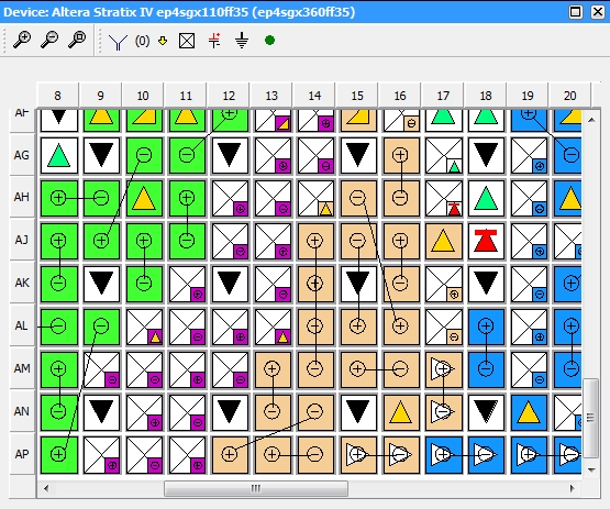
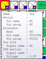
Fuzzy matchingAs described earlier, the FPGA and PCB names will often differ from each other. Other differences can be introduced by the way the tools handle bus indices like '(', '[' or '<', and bus signals like (bus[2]) and expanded signals (bus_2). IO Checker remaps all bus indicators ('('and '[') to a single indicator ('<') and the fuzzy name comparator ignores underscores in names. Alternate device supportA secondary device (within the same family) can be specified as an alternate (migration) device. The device view will show both pin types when they differ on both devices. If no FPGA pin file is present, IO Checker will verify that the connected PCB signal is correct for both devices.
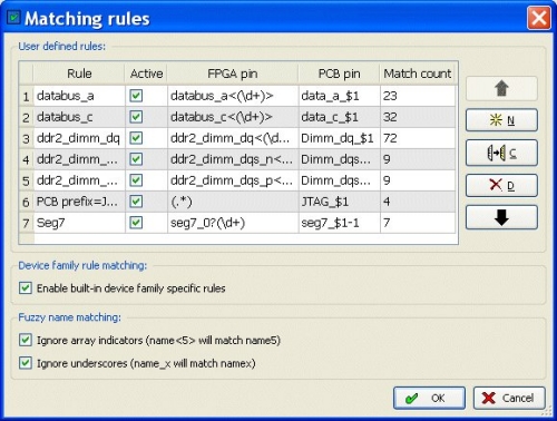
Rule based matchingRules can be created automatically by the Rule Generator or manually by the user. These rules allow non-matching names to match. The mapping rules allow the use of regular expression to quickly match related names.
Default rules can be defined in the user settings so they can be easily reused for other projects. Power rulesAnother mistake sometimes made when placing an FPGA on a PCB is related to the power pins. The FPGA IO banks can require a different VCC voltage than the FPGA core voltage and these banks can be programmed for different IO standards requiring a different voltage supply. IO Checker extracts the required power information from the FPGA vendor pin list file and compares them with the voltage information from the PCB netlist. This helps prevent mistakes that can result in fried ICs!. Intelligent power extraction from decoupled power suppliesIO Checker can now recognize secondary power nets which feed (analog) power pins of an FPGA and are connected through a decoupling circuit (inductor and capacitors to GND) to the main power supplies on the PCB. A warning message is generated when decoupled power nets indicate different voltage strength. VerificationVerification has improved in several areas. When a pin is marked as a power or ground pin (in the pin file) IO Checker will only verify the pin is connected to the right voltage and ignore the net name. If an alternate device is specified (without pin file) the pin verified for the combined behavior. Extra checks for power and ground have been added when only a PCB netlist is present. Signal ViewRequired voltages for power pins are shown between <> to distinguish them from IO Standards. The same is done for signal names in the pin file column when they relate to a pin signal name instead of specific user IO signal. An icon depicting its nature is shown for PCB nets that fall into one of the predefined categories (single/multi pullup, single/multi pulldown, decoupling, dangling, unconnected). Search widgetsThe blocking search widgets have been replaced with a non-blocking version making it easier to search for pins or signals.
Extended signal name extractionAdditional signal information is shown in the PCB column for nets that are decoupled with a single resistor. Matching rulesThe rule matching dialog has been extended with a 'Generate' button, making the 'New rules' dialog obsolete. An extra column is added showing an icon when the rule is new. Undo/Redo buttons allow you to fix any errors you made in the rules. TCL command-line interfaceThe TCL interface has been extended with functions to extract information about pins from both the IO Checker database and the FPGA pin file. These functions make it possible to extend and customize the IO Checker functionality. Automatic PCB netlist format recognitionIO Checker can automatically determine the format of the netlist specified based on the file extension and known keywords that are found in the file. Company corporate data directory and settingsCompany global settings like used FPGA vendor, PCB vendor and default matching rules can be defined and stored on a directory that each designer can use to retrieve the standard settings. Tooltips on PCB signal namesA tooltip with all connected pins of the associated net will be shown when the tooltip is activated in the PCB signal column. User accepted power mismatchesThe designer can manually accept a power mismatch and mark as correct. The error flag will be replaced by a user accepted flag. The user accepted flag will be removed when the design data is re-importing with different power values. HTML GenerationThe HTML documentation function allows you to export the IO Checker signal view into an HTML document. FPGA Devices
Schematic capture / PCB Systems
Operating Systems
License Configuration
Click here to download EASE, HDL Companion, or IO Checker Would you like a quick walk-through of IO Checker? Please contact our sales department by phone 540-953-3390 or email [email protected]. |
|
|

