4.2 Register and Latch Equations |

|

|
|
4.2 Register and Latch Equations |
|
|
4.2 Register and Latch Equations |
|
|
|
4.2 Register and Latch Equations |
|
|
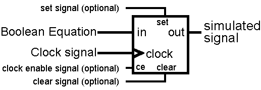
A signal can be defined as a register or latched equation similar to a cell in an FPGA. The Boolean equation is the input to a register or latch and the model is determined by the options that you choose. These signals will properly export as VHDL and Verilog models rather than just straight waveform stimulus. The following is a diagram of the model defined in the Signals Properties dialog.
Using a Registered or latched Equation:
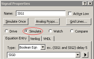
•Double-click on a signal name to open the Signal Properties dialog and enter an equation into the Boolean equation box and select the Simulate button. •The Boolean equation can either be the name of the input signal or an entire equation. |
|
•To activate the register or latch model, you must choose a Clock signal and an Edge/Level type. The clock can be any signal in the diagram. |
•For a Register circuit choose neg, pos, or both to define the triggering edge. •For a Latch circuit choose either low or high level latching |
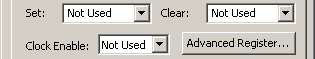
•The Set, Clear, and Clock Enable are optional signals. If "Not Used" is chosen for a line, then that line is not modeled. |
|
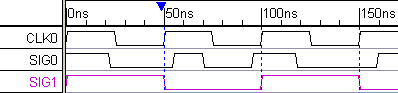
•Below is an example. SIG1 is the output of a positive edge triggered register. The CLK0 is the input clock and SIG0 is the signal that is being registered. The blue lines are grid lines placed on the positive edge to the clock to show the sampling points (See Section 2.3: Grid Lines on Clocks and Signals).
Altering the Register or Latch Models:
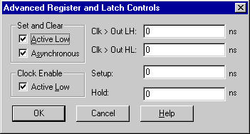
•Pressing the Advanced Register button opens the Advanced Register and Latch Controls dialog and has the controls for the timing options for this signal's register or latch model. •The Set and Clear lines can be active low or active high. The can also be asynchronous so that a change on the line immediately effects the output. Or they can be synchronous so that the output does not change until the next active level of the clock. |
|
•Clock Enable line can be either active high or low. •Clock to Out boxes specify the delay from the triggering of the clock signal to a change on the output edge. This setting supports both a Low to High model and a High to Low model. •Setup specifies the time for which the input must be stable before the clock-triggering event. If a min/max timing parameter is entered, Setup will use the min time. Any violations of this setup time will be reported to the simulation log in the Report window. •Hold specifies the time for which the input must remain stable after the clock-triggering event. If a min/max timing parameter is entered, Hold will use the min time. Any violations of this hold time will be reported to the simulation log in the Report window. •The global defaults for this dialog can be defined using the Options > Diagram Simulation Preferences menu. |
Replacing SynaptiCAD's Register or Latch Models:
The files SynaptiCAD\hdl\wavelib_ModelType.v contain the generic register and latch models.The ModelType is determined by the Flip-flop library box Options>Diagram Simulation Preferences dialog. Be very careful and make copies if choose to edit or replace these models.